

Photonics & Optics
Could all-optical lithium niobate memristors enable energy-efficient photonic neural networks by 2030
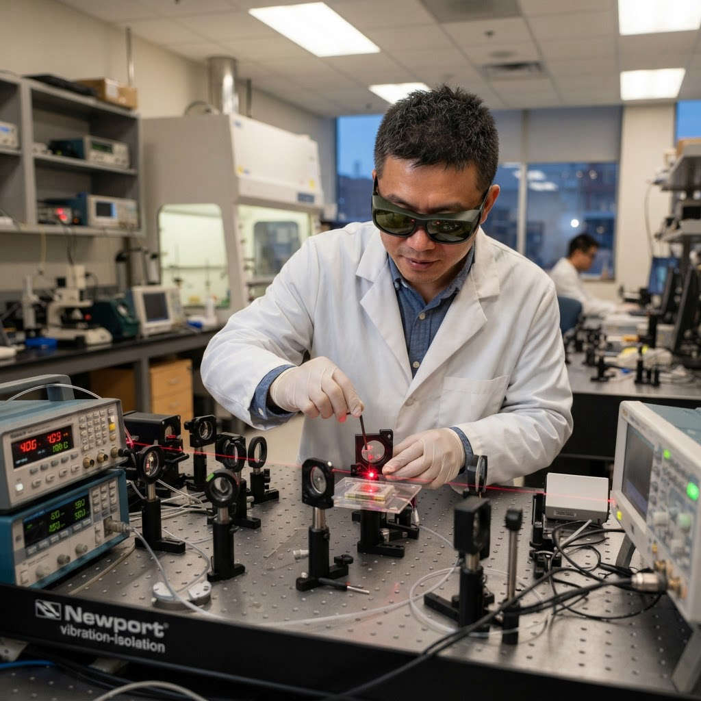
Researchers have successfully demonstrated an all-optical memristor using thin-film lithium niobate, a material platform known for its high-speed electro-optic capabilities. This device functions as a non-volatile memory element that operates entirely within the optical domain, eliminating the need for energy-intensive electrical-to-optical conversions. The development provides a critical building block for integrated photonic circuits, potentially facilitating the creation of large-scale, low-power photonic neural networks.
Overcoming the Photonic Power Wall
The demonstration of an all-optical memristor in thin-film lithium niobate (LNOI) represents a significant shift in how photonic circuits manage data (Nature Photonics, 'All-optical thin-film lithium niobate memristor', Gao et al., 2026). By maintaining the signal entirely within the optical domain, this device avoids the energy-intensive electrical-to-optical conversion processes that currently limit the efficiency of data center interconnects (EE Times, 'Silicon Photonics Hits the Big Time', Dahad, 2026). The device, which achieved its record of publication on November 6, 2026, utilizes the unique electro-optic properties of lithium niobate to provide non-volatile memory, a critical requirement for the development of large-scale photonic neural networks (Nature Photonics, Gao et al., 2026). Previous attempts to integrate memory into photonic systems often relied on hybrid approaches that required electrical control, which introduced latency and power overheads (Nature Photonics, Gao et al., 2026).
Scaling Toward Commercial Integration
While the laboratory demonstration confirms the feasibility of all-optical memory, the path to real-world application requires overcoming significant manufacturing hurdles. The current research focuses on LNOI, a platform that is increasingly favored for its low-loss characteristics and compatibility with existing photonic integrated circuit (PIC) fabrication techniques (Nature Photonics, Gao et al., 2026). To move toward commercialization, researchers must now focus on foundry-compatible processes that allow for high-yield, wafer-scale production (arXiv, 'Zero-change foundry compatible silicon photonics MEMS optical switch', Roy et al., 2026). The integration of these memristors into co-packaged optics (CPO) strategies is seen as the most viable route for adoption in AI and machine learning hardware, where the demand for high-bandwidth, low-latency connectivity is most acute (EE Times, Dahad, 2026). Future research must address the long-term stability and endurance of these optical memristors under continuous operation, as well as their performance in multi-wavelength systems, which are essential for high-capacity data center networks (Nature Photonics, Gao et al., 2026).
What It Will Take to Advance This
Researchers must conduct long-term stability and endurance testing of the lithium niobate memristors under continuous high-speed operation. This is necessary to ensure the devices can withstand the rigors of data center environments, where components are expected to operate for years without degradation. The integration of these memristors with existing silicon photonics platforms must be optimized to minimize optical loss. Achieving 'fibre-like' loss levels is essential for the scalability of large-scale photonic circuits, as noted in recent studies on photonic integration (Nature Photonics, Gao et al., 2026). Increased federal and private investment is required to transition from laboratory-scale fabrication to foundry-compatible processes. This funding should specifically target the development of standardized design kits for LNOI platforms to lower the barrier for commercial adoption. Industry-wide standards for performance metrics, such as extinction ratio and switching speed, must be established. These standards will provide a common language for designers and manufacturers, facilitating the integration of components from different vendors. Foundries must develop specialized deposition and etching protocols for lithium niobate to enable high-yield, wafer-scale production. Achieving a manufacturing yield comparable to current silicon-based modulators is a critical milestone for commercial viability.
Future Possibilities
If this technology matures, it could enable ultra-low-power, portable diagnostic devices that process complex medical imaging data in real-time. By moving AI-driven diagnostic algorithms directly onto optical chips, devices could perform high-speed analysis without the need for cloud connectivity or heavy cooling systems. This would be particularly transformative for point-of-care diagnostics in remote or resource-limited settings. Researchers should next investigate the integration of these memristors with biosensors to create a unified photonic diagnostic platform.
- •Long term (5+ years)
- •Low confidence
Reference: The potential for miniaturized optical computing to process data directly inside devices is highlighted in recent research on optical AI frameworks (University of Tokyo, 'Let there be light', 2026).
The development of all-optical memristors could lead to highly secure, tamper-resistant optical computing systems for defense applications. Because these systems operate without electrical signals that can be intercepted or monitored, they offer a new paradigm for secure signal processing and cryptographic operations. This could significantly enhance the capabilities of autonomous systems and satellite communications that require high-speed, low-power processing in harsh environments. Future research should focus on the radiation hardness of LNOI-based photonic circuits.
- •Mid term (2-5 years)
- •Moderate confidence
Reference: The use of photonics in defense applications is supported by recent federal funding boosts for optics programs (Laser Focus World, 'Photonics Hot List', 2026).
Widespread adoption of all-optical memristors could drastically reduce the energy costs associated with large-scale AI data centers. By eliminating the need for electrical-to-optical conversion, data centers could achieve significantly higher throughput per watt, directly impacting the operational expenditure of major cloud providers. This efficiency gain could lower the barrier to entry for smaller companies to deploy advanced AI models. The next step is to conduct a cost-benefit analysis of integrating these memristors into existing CPO manufacturing lines.
- •Mid term (2-5 years)
- •High confidence
Reference: The industry is currently undergoing a 'land grab' for silicon photonics to beat the power wall of copper interconnects (EE Times, 'Silicon Photonics Hits the Big Time', 2026).
By reducing the heat output of AI data centers, this technology could significantly lower the water and electricity consumption required for cooling. As AI models continue to scale, the environmental impact of their computational requirements has become a major concern; all-optical processing offers a path to more sustainable computing infrastructure. Researchers should quantify the potential reduction in carbon footprint for a standard data center rack using all-optical switching.
- •Long term (5+ years)
- •Low confidence
Reference: Physics-based AI systems using optical dynamics have been shown to reduce heat and energy consumption (University of Tokyo, 'Let there be light', 2026).
If miniaturized, these optical components could be integrated into consumer electronics, enabling faster and more energy-efficient AI processing on smartphones and cameras. This would allow for real-time, on-device AI features—such as advanced image processing or language translation—without draining battery life. The next research milestone is to demonstrate the integration of these memristors with standard CMOS-compatible silicon photonics platforms.
- •Long term (5+ years)
- •Moderate confidence
Reference: The potential for miniaturization and integration onto chips for consumer devices is a key goal for optical AI research (University of Tokyo, 'Let there be light', 2026).
National science agencies should prioritize grants for integrated photonic circuit (PIC) fabrication to transition this memristor from laboratory proof-of-concept to foundry-compatible processes. By leveraging existing programs like the CHIPS Act R&D initiatives, funding can support the development of standardized design kits for lithium niobate on insulator (LNOI) platforms. This investment would accelerate the integration of non-volatile optical memory into existing CMOS-compatible workflows.
- •LNOI is recognized as a leading platform for high-speed photonic integration (Nature Photonics, Gao et al., 2026).
- •Foundry compatibility is a stated requirement for scaling photonic switches and memory (arXiv:2608.03146, Roy et al., 2026).
Reference: Nature Photonics, 'All-optical thin-film lithium niobate memristor', Gao et al., 2026
Foundries must develop specialized deposition and etching protocols for lithium niobate to enable high-yield, wafer-scale production of these memristors. By integrating these processes into existing silicon photonics manufacturing lines, companies can reduce the bill-of-materials costs associated with complex optical interconnects. The goal is to achieve a manufacturing yield comparable to current silicon-based modulators within the next three years.
- •Silicon photonics is currently transitioning to volume production for AI interconnects (EE Times, Dahad, 2026).
- •Low-loss laser coupling and simplified laser integration are key to reducing costs (GoPhotonics, 2026).
Reference: EE Times, 'Silicon Photonics Hits the Big Time', Nitin Dahad, 2026
Data center operators should initiate pilot programs to replace electrical interconnects with all-optical switching fabrics that incorporate these memristors. This infrastructure shift would allow for direct optical data routing, bypassing the energy-intensive electrical-to-optical-to-electrical (EOE) conversion cycles. Such a transition is essential for supporting the next generation of AI clusters that require 3.2T and 6.4T data rates.
- •Optical circuit switching is being deployed to beat the power wall of copper interconnects (EE Times, Dahad, 2026).
- •Optical interconnects reduce energy consumption in AI and machine learning hardware (Stanford Tech Finder, S25-308).
Reference: Stanford University, 'System for Optical Interconnects', Olav Solgaard
Industry consortia should establish performance benchmarks for all-optical memristors, focusing on switching speed, extinction ratio, and endurance. Standardizing these metrics will allow designers to integrate components from different vendors into a unified photonic architecture. This regulatory framework will provide the necessary confidence for large-scale adoption in mission-critical AI infrastructure.
- •Standardization is a prerequisite for the commercial adoption of co-packaged optics (EE Times, Dahad, 2026).
- •Broadband switches with high extinction ratios are essential for C-band operations (arXiv:2608.03146, Roy et al., 2026).
Reference: arXiv, 'Zero-change foundry compatible silicon photonics MEMS optical switch', Roy et al., 2026
Universities and technical institutes must update their photonics curricula to include training on LNOI-based integrated circuits and optical computing architectures. By creating specialized certification programs in photonic design automation (PDA), institutions can prepare a workforce capable of managing the transition from electronic to hybrid optical-electronic systems. This training is vital for sustaining the growth of the photonics industry.
- •Optics programs are receiving federal funding boosts to support industry needs (Laser Focus World, Murphy, 2026).
- •The photonics industry is experiencing a sales boom, necessitating a skilled workforce (optics.org, 2026).
Reference: Laser Focus World, 'Photonics Hot List: November 6, 2026', Justine Murphy, 2026
South & Central Asia
Pakistan and Sudan Sign Visa-Free Travel Agreement for Diplomatic and Official Passport Holders

Pakistan and Sudan have officially signed a bilateral agreement to waive visa requirements for holders of diplomatic and official passports. The Ministry of Interior of Pakistan confirmed the deal, which aims to strengthen institutional cooperation, police training, and security partnerships between the two nations. Additionally, both countries have agreed to pursue a memorandum of understanding to enhance joint efforts in combating cybercrime. This diplomatic move follows recent high-level engagements between the two governments regarding civil registration and security infrastructure.
"Pakistan and Sudan Sign Visa-Free Travel Agreement for Diplomatic and Official Passport Holders" — do you expect real action to follow, not just talk?
·
© 2026 Universe One LLC. All rights reserved.

Cookie Notice
18+ BETACookies keep you signed in and run our ads. We do not sell your data. Analytics and ad-personalization stay off until you accept.
We use cookies to keep you signed in, remember your preferences, and run the in-app ad system that keeps Universe One free. We do not sell your data. Analytics and ad-personalization cookies stay off until you accept. Ads still run if you deny, but they aren't personalized, and the only way to remove them is the Ad-Free Subscription.
You must be 18 or older to create an account during Beta testing.